Services
We provide co‑funded access to infrastructure and specialized skills‑development programs related to semiconductor technologies. Through access to a regional and European network of experts and facilities we enable SMEs and start-ups as well as large companies and universities to innovate faster, more cost‑effectively, and with reduced risk.

The services are co-funded according to the Programme for the State-Aid Support (GBER). The public call will be posted in our News section once it is officially published by the Ministry.
Skills Development

CROCCS offers specialized skills‑development programs and workshops related to chip design and electronics engineering. Below is a preselection of available training topics. As we continue expanding our portfolio, you are welcome to reach out with interest in additional topics.
Demonstrator development is a service offered to start-ups and SMEs to bring their ideas to life. It supports users in designing their own chip, with guidance at every stage of the process—from design to fabrication and characterization. The resulting demonstrator provides a tangible proof of concept, enabling early evaluation of the benefits of chip design and identification of potential risks.
Trainings
- Chip design (Analog IC design, Digital IC design and verification, Mixed-signal IC design, Chip design using open-source tools)
- Characterization (Nano- and micro-imaging and related analysis, electrical and thermal characterization of semiconductors under extreme conditions)
- Processing (Thin film deposition and microstructuring)
- Neuroelectronics (Principles and Applications of Neuroelectronic Interfaces in Medical Bionics, Preparation and Use of In-Vitro Neural Cultures for Testing Neuroelectronic Interfaces)
- Electronic systems (Power electronic system design)
Demonstrator development
- Service for ASIC (Application Specific Integrated Circuit) development
Support in Developing Semiconductor Solutions
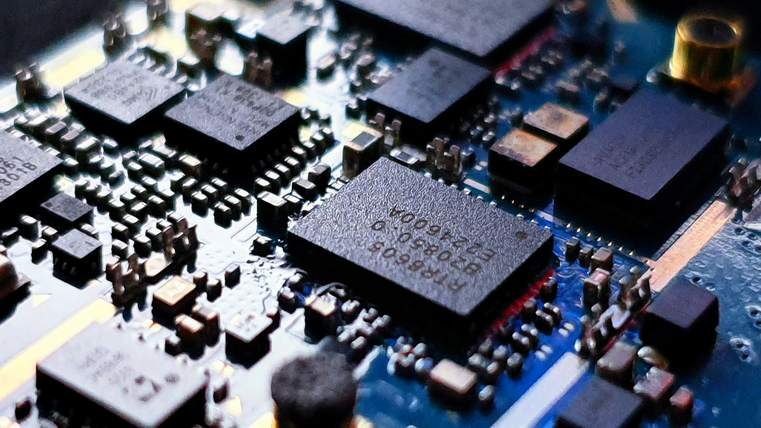
CROCCS deliver comprehensive infrastructure and expert support for your development of innovative semiconductor-based solutions. An indicative list of available support services is provided below.
Processing services
- Ion beam implantation (Broad or microbeam implantation of elements 1<Z<92 in the different substrates at RT or elevated temperature (up to 800°C). Implantation areas from few um^2 up to cm^2, with fluences up to 10^16 ions/cm^2)
- Deposition on thin film by magnetic sputtering (Deposition of thin films using magnetron sputtering technology on wafers)
- Clean room access (Access to clean room equipment (LPCVD/PECVD deposition of amorphous/crystalline silicon: p/n-doping, MOCVD deposition of ZnO thin films: p/n-doping, DC magnetron sputtering of metals; using mask aligner, photolithography, RCA cleaning, RIE etching, laser wafer cutting, time resolved PL characterisation (up to 100 ps)).
- Electron beam lithography (Maskless lithography using an electron beam for drawing custom patterns on devices and designing contacts for measurements)
- Microstructuring by optical lithography (Definition of masks for optical lithography for single- or multi-layer processes; with the use of mask-aligner and supporting equipment (spinner, heater, fume hood) and chemicals, single- or multi-stage microstructuring of thin films.)
Material characterization
- Electroluminescence and photoluminescence (Measurement of the electroluminescence and photoluminescence of semiconductor materials and devices. Different sample holders are available. Moreover, several lasers for optical excitation covering the Group IV semiconductor devices and wide-bandgap semiconductors (SiC, GaN). The temperature range is from He (ca 10K) up to 500K.)
- TOF-ERDA (Quantitative analysis of thin film samples (~ 400 nm) with flat surfaces, and analysis of depth profiles of elements 1<Z<92, with isotope resolution up to mass 40)
- RBS and PIXE (Quantitative analysis of samples by PIXE (Particle Induced X-ray Emissions) and RBS (Rutherford Backscattering Spectroscopy) of basic elements and trace elements 3<z<92, with a beam of 2MeV protons and a beam diameter of 3 to 5 mm, or ~ 1 µm dimensions (scan up to 1x1mm^2 area)
- SAXS and XRR (Enables determination materials crystalline structure, layer thicknesses, size, shape and arrangement properties of nanostructures within material and similar structural properties)
- Quantum efficiency measurement (Number of generated excitons per single incident photon)
- Micro-Raman spectroscopy (Characterisation of structural properties of semiconductor materials with spatial resolution of 0.5 µm including mapping of surface or cross sections of deposited layers or devices.)
- X-ray diffraction (Characterisation of structural properties of semiconductor materials by X-ray diffraction.)
- SEM and EDS (Morphological, structural and chemical characterization of materials and devices on micro/nanoscale and chemical characterization by EDS-energy dispersion spectroscopy)
- AFM (Nano-imaging of surfaces with the possibility of determining hardness on the nanoscale)
- QD PPMS (Measuring physical properties of materials and devices (electric transport, heat capacity, DC magnetization, torque magnetometer, multifunctional probe) in temperature range 1.9K-400K)
- Profilometer (Surface topography measurement system using non-contact, white light interferometry)
- Transport measurements (Measurements of electron/ion transport in materials, batteries and devices in specific environment (oxygen-free, moisture-free, ionic liquid, etc.)
Device and circuits characterization
- Complete electrical characterization (Characterization of semiconductor devices covering wide range of temperatures (2K – 400K), magnetic fields (up to 12.5 T), thermal conductivity measurements, etc.)
- On-wafer DC and RF measurements (S-parameter measurements up to 8,5 GHz, DC characteristics are measured using precise SMUs)
- Automated characterization of integrated circuits (Versatile characterization of analog IC using PXI system with high-precision A/D and D/A converters, high-speed pattern generators, SMU and signal generators)
- Optical characterization of photosensors (The measurements of spectral sensitivity and/or time response of various discrete or integrated photo sensitive devices. Available sources include Xenon lamp, LED sources and various CW and pulsed lasers)
- Basic laboratory measurements in time and frequency domain (4-port VNA measurements up to 8,5 GHz, TDR/TDT min. rise time equal to 17,5 ps, TLP measurements with min. pulse duration of 10 ns, DC characterization, AC characterization, freq. spectrum analysis)
Testing
- Type tests (EMC Directive, RED Directive, LV Directive, Environmental directives (vibro&shock, climatic)
- PHIL (Testing semiconductor components, modules and power electronics circuits using the hardware-in-a-loop approach)
- Power electronics (Double-pulse method, switching losses, switching delay time, gate driver protection functions, efficiency of the power converters (<1000 V) up to power of 40 kW using precise power analyzer that employs fluxgate current sensors up to 700 Arms)
- Reliability (EMC (Temperature characterization of ICs combined PXI system, EMC precompliance testing: TEM cell, IC-Stripline, conducted emission testing, DPI method conducted immunity testing)
- Temperature/heat investigation (Temperature/heat investigation of ICs, PCBs and other electronics/device systems on a temperature setup using FLIR A6753 camera (from -10C to 350C) and 1x and 5x lenses.
Consulting services
CROCCS provides comprehensive support to help innovators assess and strengthen their ideas, validate their technical potential, and identify the skills and infrastructure needed to advance them.
Feasibility study
Expert Guidance
Access to finance support/Technology and knowledge transfer support
Gateway to European Semiconductor Ecosystem
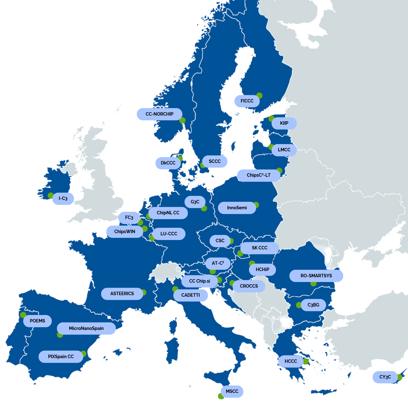
Whenever a specific training or support service is not available within CROCCS, our clients benefit from direct access to the wider ecosystem of European Network of Chips Competence Centres, Design Platforms, and Pilot Lines—unlocking cutting‑edge expertise, facilities, and development opportunities.
ENCCC (European Network of Chips Competence Centres)

No single Chips Competence Centre (CCC) can cover all services across semiconductors value chain. As your gateway to the ENCCC, CROCCS connects you with the right partners and supports your needs beyond our in-house capabilites.
Pilot Lines
Fully Depleted SOI and Advanced Memory for European Semiconductors
FAMES strengthens Europe’s semiconductor ecosystem by advancing high-performance, energy-efficient, and environmentally sustainable chip solutions. Specializing in FD-SOI (Fully Depleted Silicon-On-Insulator) technologies at 10 nm and 7 nm nodes, it also integrates embedded non-volatile memories (eNVMs).
Sustainability is at the core, with resource optimization, circular-economy practices, and waste minimization across the entire technological process — from chip design to manufacturing — supporting the industry’s pursuit of net-zero emissions by 2050.

Advanced Packaging and Heterogeneous Integration for Electronic Components and Systems
APECS focuses on cutting-edge packaging and heterogeneous integration technologies, going beyond conventional system-in-package methods. It offers services, capabilities, and training for European companies and research organizations to integrate and package chiplets and other advanced electronic components into novel electronic systems.
Bringing together the expertise of ten partners from eight European countries, APECS covers end-to-end design and pilot production capabilities — from characterization and testing to demonstrators that validate new technologies — accelerating the transfer of ideas from research to practical, scalable manufacturing solutions.
Pioneering Beyond-2nm System-on-Chip Innovation
NanoIC accelerates the development of next-generation SoC (System-on-Chip) technologies beyond the 2 nm node. It provides advanced R&D infrastructure and state-of-the-art tools for startups, SMEs, and research institutions.
With early-stage Process Design Kits (PDKs) and prototyping capabilities, NanoIC enables risk mitigation and early validation of new semiconductor features—fueling innovation in materials and fabrication modules.
Photonics Integration Pilot Line for Europe
PIXEurope is a leading European initiative advancing photonic integrated circuits (PICs). Coordinated by ICFO (Barcelona) with 20 partners from 11 countries — Austria, Belgium, Finland, France, Ireland, Italy, Poland, Portugal, Spain, the Netherlands, and the United Kingdom — the pilot line supports the industrialization of cutting-edge photonics technologies.
By bridging research and industry, PIXEurope promotes widespread adoption of integrated photonics in fields such as communications, AI, sensing, healthcare, and advanced semiconductor systems—strengthening Europe’s global competitiveness.

Wide Bandgap Materials for Power Electronics
Coordinated by CNR-IMM (Italy), the WBG Pilot Line focuses on developing new, high-performance and durable semiconductor materials for power electronics. The consortium brings together research organizations and universities from across Europe, working on wide-bandgap materials such as gallium nitride and silicon carbide, with gallium oxide and aluminum nitride prioritized in later phases.
The pilot line aims to boost the efficiency of Europe’s advanced power devices and establish a robust, European value chain—enabling new product families with superior features currently unmet by the market.
Design Platform
The European Chips Design Platform EuroCDP
EuroCDP is being developed to help startups, SMEs, research teams, and fabless innovators bring microchip ideas to life faster. The platform will provide easy access to everything needed for chip design and development – from design tools, IP, and expert support to prototyping, fabrication, packaging, testing, training, funding, and startup-focused programmes.
By bringing these services together in one place, EuroCDP will serve as a one-stop platform for chip design in Europe. It will support users throughout the entire journey, from early concept development to a finished microchip, whether for proof-of-concept projects or market-ready innovations.
EuroCDP will be available to organisations from EU Member States and countries participating in the Chips Joint Undertaking. The first services are expected to be launched in early 2026, with additional offerings to be added as the platform develops further.
Contact us
To help us understand your needs and connect you with the right experts and services, please provide the following information.